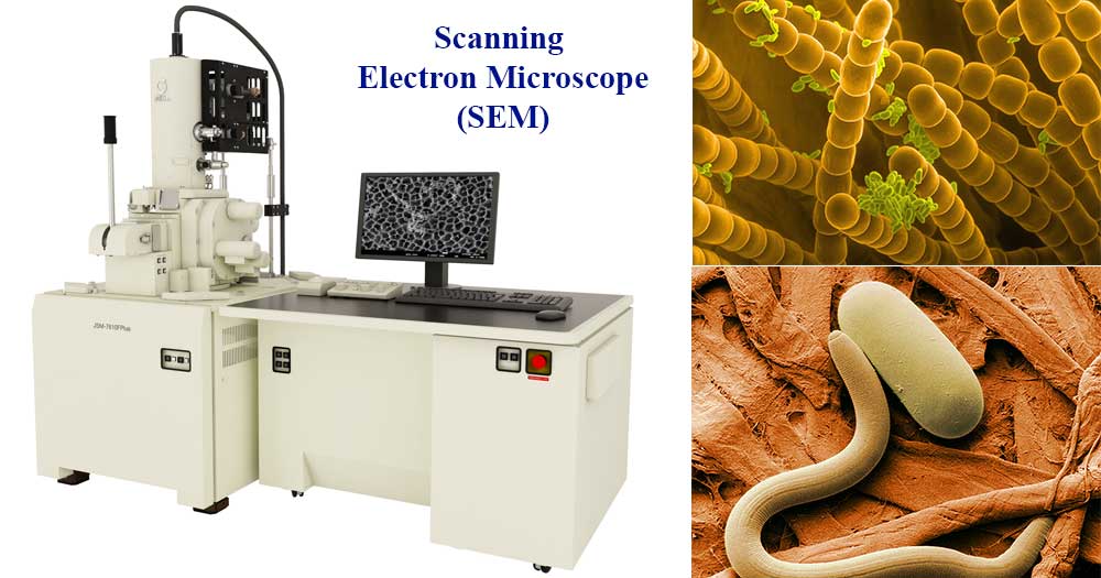
المجهر الالكتروني الماسح scanning electron microscope
*
The Principle of the Scanning Electron Microscope
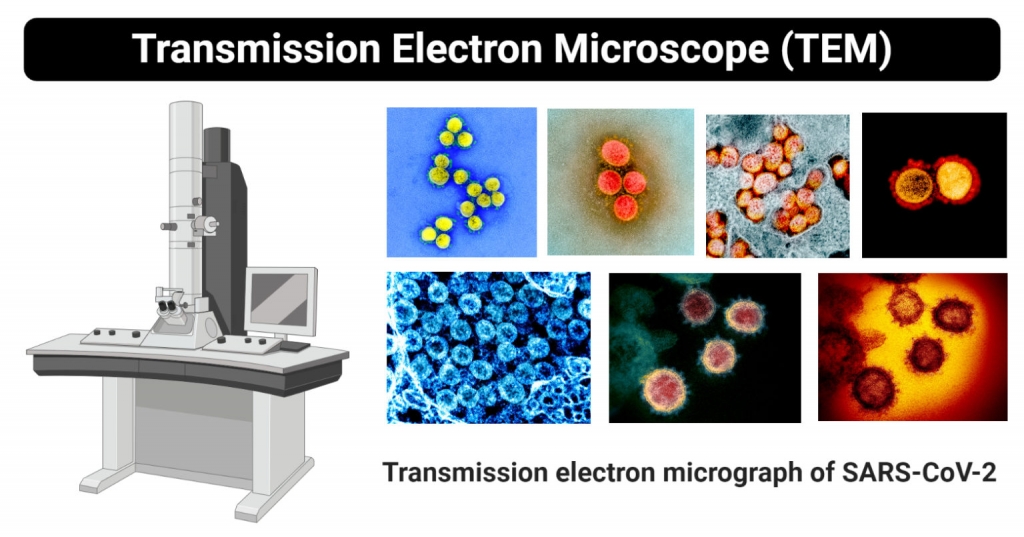
Unlike the Transmission Electron Microscope which uses transmitted electrons, the scanning electron Microscope used emitted electrons.
The Scanning electron microscope works on the principle of applying kinetic energy to produce signals on the interaction of the electrons. These electrons are secondary electrons, backscattered electrons and diffracted backscattered electrons which are used to view crystallized elements and photons. Secondary and backscattered electrons are used to produce an image. The secondary electrons are emitted from the specimen play the primary role of detecting the morphology and topography of the specimen while the
backscattered electrons show contrast in the composition of the elements of the specimen.
How does the Scanning Electron Microscope (SEM) work *

- The source of the electrons and the electromagnetic lenses are from tungsten filament lamps that are placed at the top of the column and it is similar to those of the transmission electron Microscope.
- The electrons are emitted after thermal energy is applied to the electron source and allowed to move in a fast motion to the anode, which has a positive charge.
- The beam of electrons activates the emission of primary scattered (Primary) electrons at high energy levels and secondary electrons at low-energy levels from the specimen surface. The beam of electrons interacts with the specimen to produce signals that give information about the surface topography and composition of the specimen.
- The specimen does not need special treatment for visualization under the SEM, even air-dried samples can be examined directly. However, microbial specimens need fixation, dehydration, and drying in order to maintain the structural features of the cells and to prevent collapsing of the cells when exposed to the high vacuum of the microscope.
- The samples are mounted and coated with thin layer heavy metal elements to allow spatial scattering of electric charges on the surface of the specimen allowing better image production, with high clarity.
- Scanning by this microscope is attained by tapering a beam of electrons back and forth over a thin section of the microscope. When the electrons reach the specimen, the surface releases a tiny staw of electrons known as secondary electrons which are then trapped by a special detector apparatus.
- When the secondary electrons reach and enter the detector, they strike a scintillator (a luminescence material that fluoresces when struck by a charged particle or high-energy photon). This emits flashes of light which get converted into an electric current by a photomultiplier, sending a signal to the cathode ray tube. This produces an image that looks like a television picture that can be viewed and photographed.
- The quantity of secondary electrons that enter the detector is highly defined by the nature of the specimen i.e raised surfaces receive high quantities of electrons, entering the detector while depressed surfaces have fewer electrons reaching the surface and hence fewer electrons enter the detector.
- Therefore raised surfaces will appear brighter on the screen while depressed surfaces appear darker.
(Parts of a Scanning Electron Microscope (SEM
The major components of the Scanning Electron Microscope include
- Electron Source – This is where electrons are produced under thermal heat at a voltage of 1-40kV. the electrons the condense into a beam that is used for the creation of ana image and analysis. There are three types of electron sources that can be used i. e Tungsten filament, Lanthanum hexaboride, and Field emission gun (FEG)
- Lenses – it has several condenser lenses that focus the beam of electrons from the source through the column forming a narrow beam of electrons that form a spot called a spot size.
- Scanning Coil – they are used to deflect the beam over the specimen surface.
- Detector – Its made up of several detectors that are able to differentiate the secondary electrons, backscattered electrons, and diffracted backscattered electrons. The functioning of the detectors highly depends on the voltage speed, the density of the specimen.
- The display device (data output devices)
- Power supply
- Vacuum system
*
- (Applications of the Scanning Electron Microscope (SEM
It is used in a variety of fields including Industrial uses, nanoscience studies, Biomedical studies, Microbiology
Used for spot chemical analysis in energy-Dispersive X-ray Spectroscopy.
Used in the analysis of cosmetic components which are very tiny in size.
Used to study the filament structures of microorganisms.
Used to study the topography of elements used in industries.
Advantages of the Scanning Electron Microscope (SEM)
They are easy to operate and has user-friendly interfaces.
They are used in a variety of industrial applications to analyze surfaces of solid objects.
Some modern SEMs are able to generate digital data that can be portable.
It is easy to acquire data from the SEM, within a short period of time of about 5 minutes.
Limitations
They are very expensive to purchase
They are bulky to carry
They must be used in rooms that are free of vibrations and free of electromagnetic elements
They must be maintained with a consistent voltage
They should be maintained with access to cooling systems
اختراعات غيرت مجرى التاريخ


من فضلك قم بكتابة تعليق لتظهر لك روابط التحميل